Mixed Signal
In this topic:
Analog-Digital Converter
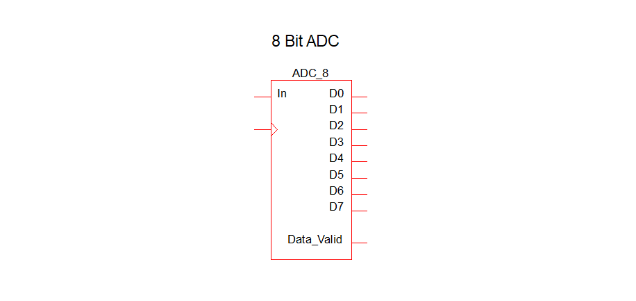
Netlist entry
Axxxx analog_in clock_in [ data_out_0 data_out_1 .. data_out_n ]
+ data_valid model_name
Connection details
| Name | Description | Flow | Type | Allowed types | Vector bounds |
| analog_in | Analog input | in | v | v, vd, i, id | n/a |
| clock_in | Clock input | in | d | d | n/a |
| data_out | Data output | out | d, vector | d | 1 - 32 |
| data_valid | Data valid output | out | d | d | n/a |
Model format
.MODEL model_name ad_converter parameters
Model parameters
| Name | Description | Type | Default | Limits |
| input_offset | Offset voltage | real | 0 | none |
| input_range | Input full scale signal range | real | 1 | none |
| twos_complement | Use 2's complement output. (default - offset binary) | boolean | FALSE | none |
| convert_time | Total conversion time | real | 1 ???MATH???\mu???MATH??? S | ???MATH???0 - \infty???MATH??? |
| min_clock | Minimum clock period | real | 500n | ???MATH???0 - \infty???MATH??? |
| data_valid_delay | Data valid inactive time | real | 100n | ???MATH???0 - \infty???MATH??? |
| in_family | See Family parameters | string | UNIV | none |
| out_family | See Family parameters | string | UNIV | none |
| family | See Family parameters | string | UNIV | none |
| input_load | Clock input load | real | 1pF | ???MATH???0 - \infty???MATH??? |
| out_res | See Output Parameters | real | 100 | ???MATH???0 - \infty???MATH??? |
| out_res_pos | See Output Parameters | real | out_res | ???MATH???0 - \infty???MATH??? |
| out_res_neg | See Output Parameters | real | out_res | ???MATH???0 - \infty???MATH??? |
| min_sink | See Output Parameters | real | -0.001 | none |
| max_source | See Output Parameters | real | 0.001 | none |
| sink_current | See Input Parameters | real | 0 | none |
| source_current | See Input Parameters | real | 0 | none |
| signed | Same as twos_complement but has integer value instead of boolean | integer | 0 | none |
| vsupply | See vsupply Parameter | real | 5 | none |
Device Operation
This is a 1-32 bit analog to digital converter. The operation of this device is illustrated by the following diagrams:
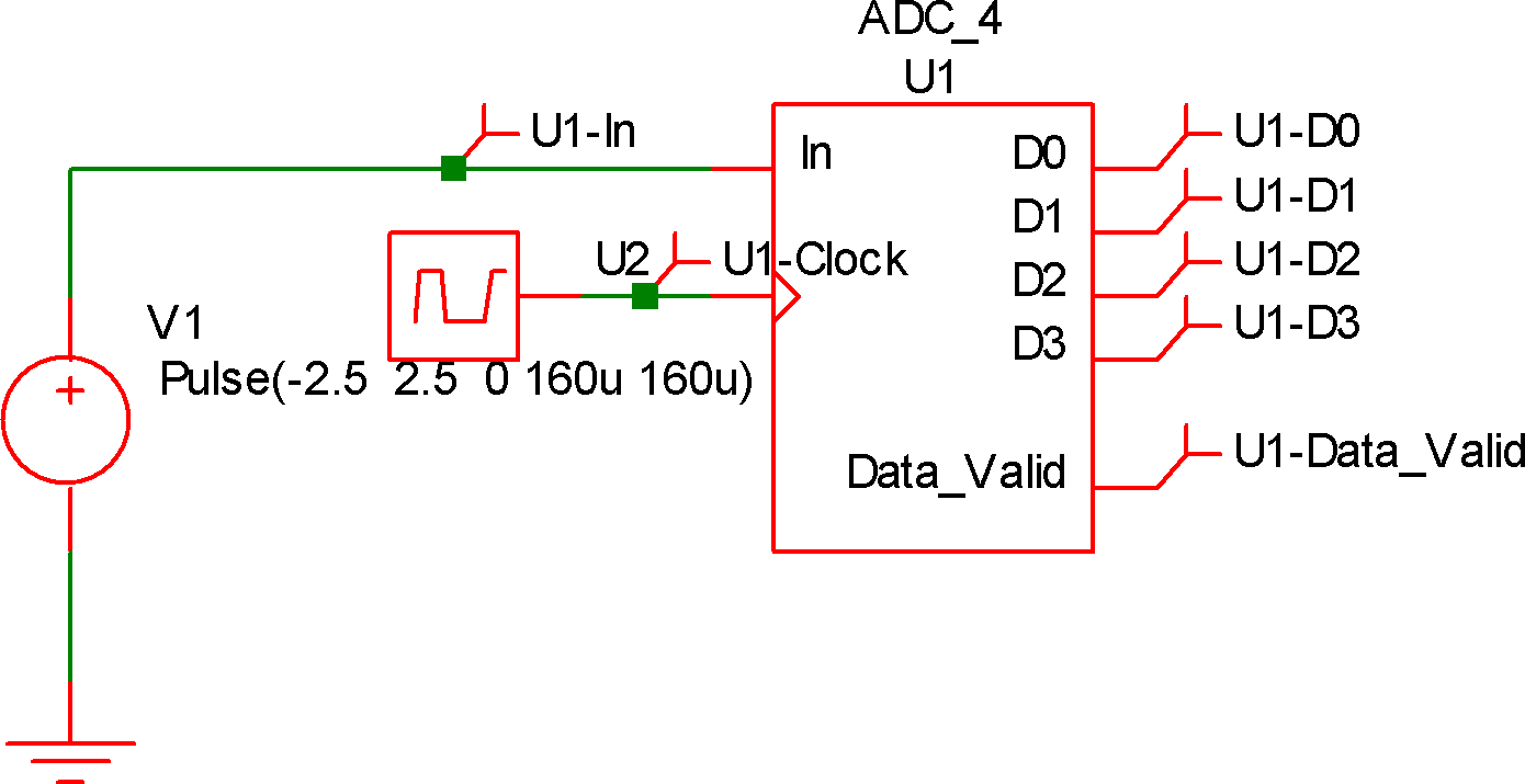
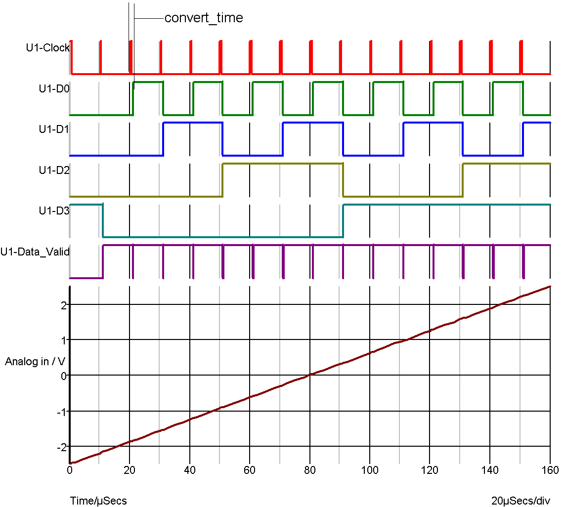
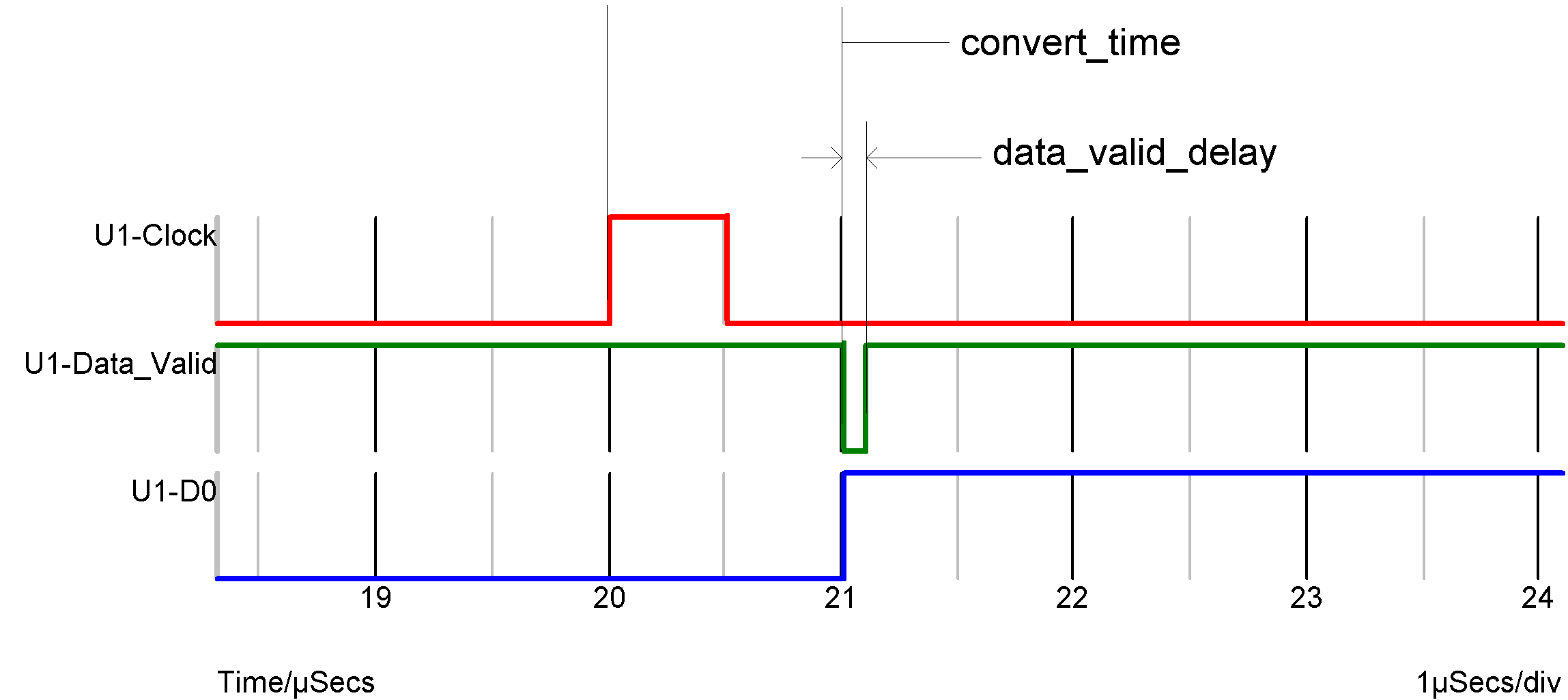
Conversion timings.
The ADC starts the conversion at the rising edge of the clock. The analog input signal is also sampled at this point. The output data changes in response to this, CONVERT_TIME seconds later. At the same time the data_valid output goes low (inactive) then high again after a delay equal to DATA_VALID_DELAY. It is possible to start a new conversion before the previous conversion is complete provided it is started later than MIN_CLOCK seconds after the previous conversion was started. MIN_CLOCK must always be less than CONVERT_TIME. If the MIN_CLOCK specification is violated, the conversion will not start.
Digital-Analog Converter
Netlist entry
Axxxx [ digital_in_0 digital_in_1 .. digital_in_n ]
+ analog_out model_name
Connection details
| Name | Description | Flow | Type | Allowed types | Vector bounds | |
| digital_in | Data output | in | d | d | 1 - 32 | |
| analog_out | Analog output | out | v | v, vd, i, id | n/a |
Model format
.MODEL model_name da_converter parameters
Model parameters
| Name | Description | Type | Default | Limits |
| output_offset | Offset voltage | real | 0 | none |
| output_range | Input signal range | real | 1 | none |
| twos_complement | Use 2's complement input. (Default is offset binary) | boolean | FALSE | none |
| output_slew_time | Output slew time | real | 10nS | ???MATH???1\text{e}^{-12} - \infty???MATH??? |
| in_family | See Family parameters | string | UNIV | none |
| input_load | Input load | real | 1pF | ???MATH???0 - \infty???MATH??? |
| sink_current | See Input Parameters | real | 0 | none |
| source_current | See Input Parameters | real | 0 | none |
| vsupply | See vsupply Parameter | real | 5 | none |
Device Operation
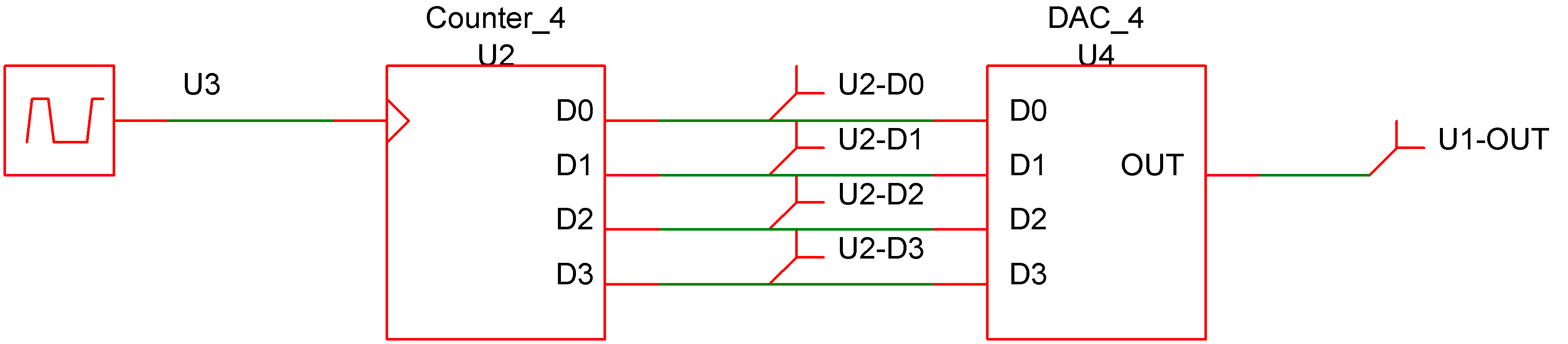
This device is a 1-32 bit digital to analog converter. Its operation is illustrated by the following diagrams.
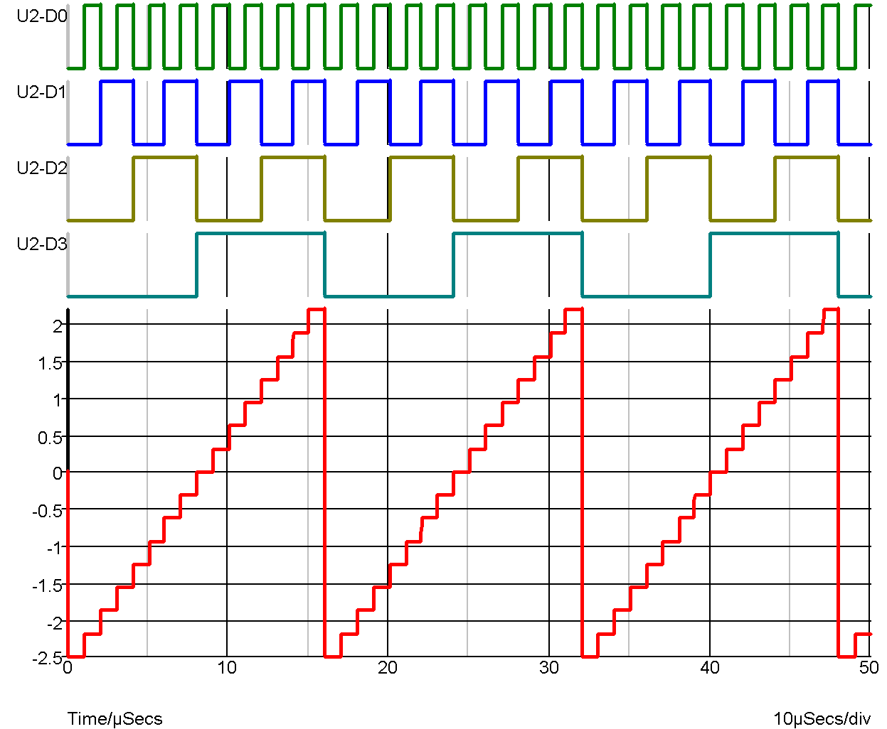 |
DAC Waveforms |
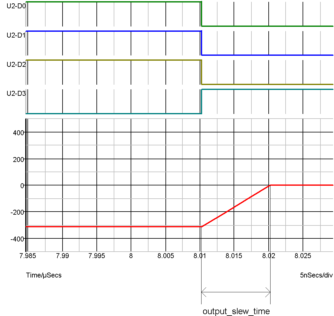 |
DAC waveforms expanded to show output slew |
The device illustrated above has the following model definition:
.model DAC_4 da_converter
+ output_slew_time 1e-08
+ output_range 5
+ output_offset 0
In offset binary mode the D-A converter produce an output voltage equal to:
-OUTPUT_RANGE/2 + OUTPUT_OFFSET + code * OUTPUT_RANGE/2 n
where n is the number of bits and code is the digital input code represented as an unsigned number between 0 and ???MATH???2^{n}-1???MATH???.
In 2's complement mode the output is:
OUTPUT_OFFSET + code * OUTPUT_RANGE/2 n
where n is the number of bits and code is the digital input code represented as a signed number between ???MATH???-2^{n/2}???MATH??? and ???MATH???2^{n/2}-1???MATH???.
Whenever the input code changes, the output is set on a trajectory to reach the target value in the time specified by OUTPUT_SLEW_TIME. UNKNOWN states are ignored. That is the input will be assumed to be at the most recent known state.
Controlled Digital Oscillator
Netlist entry
Axxxx cntl_in out model_name : parameters
Connection details
| Name | Description | Flow | Type | Allowed types | |
| cntl_in | Control input | in | v | v, vd, i, id | |
| out | Output | out | d | d |
Instance Parameters
| Name | Description | Type |
| init_phase | Initial phase | real |
Model format
.MODEL model_name d_osc parameters
Model parameters
| Name | Description | Type | Default | Limits | Vector bounds | |
| cntl_array | Control array | real vector | N/A | none | ???MATH???2 - \infty???MATH??? | |
| freq_array | Frequency array | real vector | N/A | ???MATH???0 - \infty???MATH??? | ???MATH???2 - \infty???MATH??? | |
| duty_cycle | Output duty cycle | real | 0.5 | 1???MATH???\mu???MATH??? -0.999999 | n/a | |
| init_phase | Initial phase of output | real | 0 | -180 - +360 | n/a | |
| rise_delay | Rise delay | real | 1n | ???MATH???0 - \infty???MATH??? | n/a | |
| fall_delay | Fall delay | real | 1n | ???MATH???0 - \infty???MATH??? | n/a | |
| phase_tol | Phase tolerance/degrees | real | 10 | 0 - 45 | n/a | |
| out_family | See Family parameters | string | UNIV | none | n/a | |
| out_res | See Output Parameters | real | 100 | ???MATH???0 - \infty???MATH??? | n/a | |
| out_res_pos | See Output Parameters | real | out_res | ???MATH???0 - \infty???MATH??? | n/a | |
| out_res_neg | See Output Parameters | real | out_res | ???MATH???0 - \infty???MATH??? | n/a | |
| min_sink | See Output Parameters | real | -0.001 | none | n/a | |
| max_source | See Output Parameters | real | 0.001 | none | n/a | |
| vsupply | See vsupply Parameter | real | 5 | none | n/a |
Device Operation
This device produces an output frequency controlled by an analog input signal following an arbitrary piece-wise linear law. The input to output frequency characteristic is defined by two parameters CNTL_ARRAY and FREQ_ARRAY. The following is an example of a .MODEL statement:
.model vco d_osc
+ cntl_array=[-1,0,1,2,3,4,5]
+ freq_array=[0,10000,40000,90000,160000,250000,360000]
The frequency characteristic described by the above example follows a square law. The two arrays CNTL_ARRAY and FREQ_ARRAY must be the same length. These define the frequency output for a given analog input.
Time Step Control
In order to control the accuracy of the phase of the output signal, this model may cut back the analog time step. At each analog time point, the required frequency is calculated and the digital output is set at that frequency. If the analog input changes by too large an amount between time points, the digital output phase could be substantially in error as the frequency is constant between analog time points. The actual error is calculated and if this exceeds PHASE_TOL, the time point is rejected and a time point at which the error will be in tolerance is estimated.
Note: This model was included with the original XSPICE code but the SIMetrix version has been completely re-written. The original did not have any phase error control and could not give accurate results unless the analog time step was artificially kept small.
Analog-Digital Interface Bridge
Netlist entry
Axxxx in out model_name
Connection details
| Name | Description | Flow | Type |
| in | Input | inout | g |
| out | Output | out | d |
Model format
.MODEL model_name adc_bridge parameters
Model parameters
| Name | Description | Type | Default | Limits |
| in_low | Maximum 0-valued analog input | real | 0.1 | none |
| in_high | Minimum 1-valued analog input | real | 0.9 | none |
| rise_delay | Rise delay | real | 1nS | ???MATH???1\text{e}^{-12} - \infty???MATH??? |
| fall_delay | Fall delay | real | 1nS | ???MATH???1\text{e}^{-12} - \infty???MATH??? |
| time_tol | Threshold time tolerance | real | 100pS | ???MATH???1\text{e}^{-12} - \infty???MATH??? |
| out_low | Used to calculate reflected static load. See text | real | 0 | none |
| out_high | Used to calculate reflected static load. See text | real | 5 | none |
| clamp_low | Clamp threshold 'ZERO' digital input. Default to out_low | real | out_low | none |
| clamp_high | Clamp threshold 'ONE' digital input. Default to out_high | real | out_high | none |
| clamp_res | Clamp minimum resistance | real | 1 | 1e-06 ???MATH???- \infty???MATH??? |
| clamp_bias | Clamp voltage | real | 0.8 | 0.2 - 2 |
| vsupply_nominal | nominal supply voltage, used to scale thresholds if vsupply parameter provided by connected digital device | real | 5.0 | ???MATH???0 - \infty???MATH??? |
| out_family | See Family parameters | string | UNIV | none |
| technology | Technology, e.g. HC, LVC etc. This has no effect on device operation. It is used by the user interface to group bridge models | string | none | |
| description | Sub-type to technology, e.g. schmitt, buffer, standard. This has no effect on device operation. It is used by the user interface to identify bridge characteristics | string | none |
Instance parameters
| Name | Description | Type | Default | Limits |
| interface_model | Model of device connected to bridge. Used to retrieve vsupply parameter of device if present. In normal operation using implicit bridge devices, this parameter is set automatically by the simulator | string | none | |
| inactive | if non-zero, device will output Hi-Z and present a 1Ohm input to ground. This parameter is used internally to create dummy instances for the purpose of analysing logic compatibility. | integer | 0 | none |
Device Operation
The analog-digital interface bridge is the main device used to connect analog signals to digital inputs. The device produces a digital signal that is in the logic '1' state when the analog input is above the high threshold (IN_HIGH) and a logic '0' state when it is below the low threshold (IN_LOW). When the analog input is in between these two states the output will be in the UNKNOWN state. The changes in state will be delayed according to the RISE_DELAY and FALL_DELAY parameters.
If the interface_model parameter is present, and the referenced model has a vsupply parameter, the input thresholds are scaled by a factor of vsupply/vsupply_nominal. This feature allows the supply voltage for each digital device to be customised
Analog input load
The analog input presents a load to its driving circuit according to the digital load that is being driven. In other words the digital load is reflected to the analog input. Both static (i.e. DC) and dynamic (i.e. capacitance) elements of the load are reflected. To accurately reflect the sink and source currents, the interface bridge needs to know the voltage levels of the device it is driving. The digital device will (usually) have a SINK_CURRENT and a SOURCE_CURRENT model parameter each of which apply at defined logic voltage levels. These levels must be specified in the OUT_LOW and OUT_HIGH parameters of the AD interface bridge model. The input is modelled by a current source in parallel with a resistor. The values of these components are calculated from the above mentioned parameters and the digital load.
Input clamp
The analog input is clamped at the voltages specified by CLAMP_LOW and CLAMP_HIGH. The clamping device has a characteristic similar but not identical to a junction diode in series with a resistance. Basically it has the characteristic of a diode up to a voltage excess of CLAMP_BIAS after which it becomes resistive with a dynamic resistance of CLAMP_RES. The diode characteristics are calculated so that the transition between the two regions is smooth.
Time Step Control - TIME_TOL parameter
Consider the following circuit and waveform
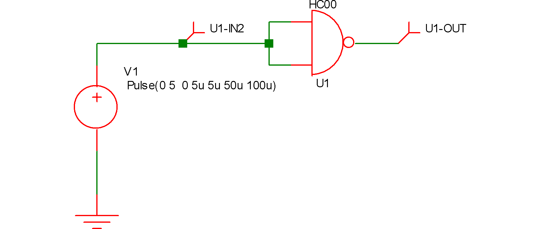
The graph shows the input and output of the NAND gate. Because the input is analog an implicit AD interface bridge will have been connected by the simulator. In the above example the parameters for this bridge have been set to:
.model HC_adc adc_bridge
+ in_low=2.1
+ in_high=2.2
+ rise_delay=1e-12
+ fall_delay=1e-12
+ out_family = "HC"
+ out_low = 0
+ out_high = 5
+ clamp_bias=0.5
+ clamp_res=10
+ time_tol=10u
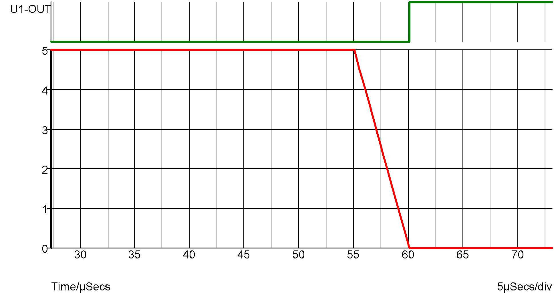
The last parameter, TIME_TOL has been deliberately set ridiculously high to demonstrate what happens without time step control on the input. The input thresholds of the HC gate are 2.1 and 2.2 volts yet the output in the above example doesn't switch until the input has reached 0V. Because there is little activity in the analog circuit, the time steps are quite large. In fact in the above example the transient timepoints are at 55uS, 55.04uS, 56.2uS, 57.8uS and 60uS. The timepoint at 57.8u is just before the 2.2 volt threshold is reached and it isn't until the next time point, 2.2uS later that the lower threshold is broken. The result is the location of the negative edge at the output is delayed by approx. 2.2uS from where it should be. The problem is that the analog system knows nothing of what is happening in the digital domain so carries on with large timesteps oblivious to the errors in the digital system.
To overcome this problem. SIMetrix features a mechanism (not in the original XSPICE system) that detects that the threshold has been passed and cuts back the time step to ensure that the digital edge occurs at an accurate point. The accuracy of this mechanism is controlled by the TIME_TOL parameter. The smaller this parameter, the more accurately the exact threshold will be hit at the expense of short time steps and longer simulation runs. TIME_TOL defaults to 100pS and in most applications this is a good choice. The following shows the result when TIME_TOL is set to the default.
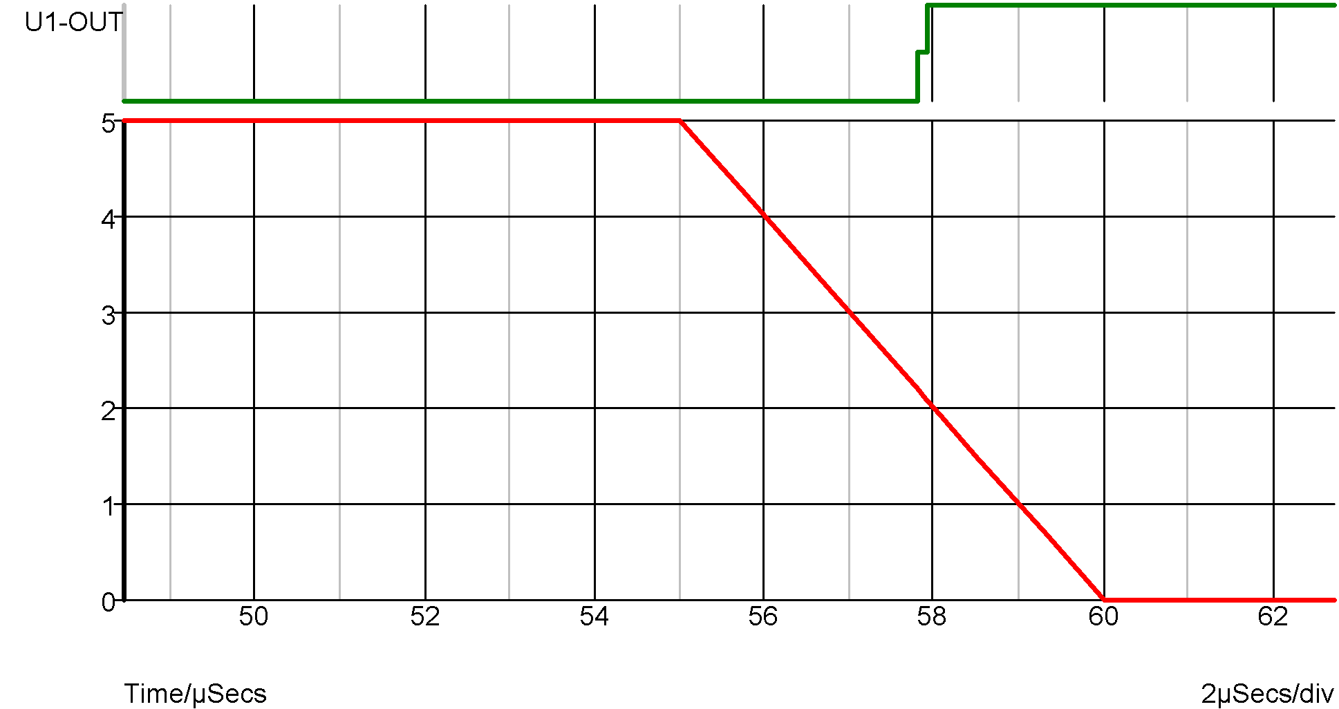
Here you can see the edge at the correct time.
The effect of not correctly simulating the threshold point has serious consequences when attempting to simulate relaxation oscillators constructed with digital inverters as the following graphs illustrate:
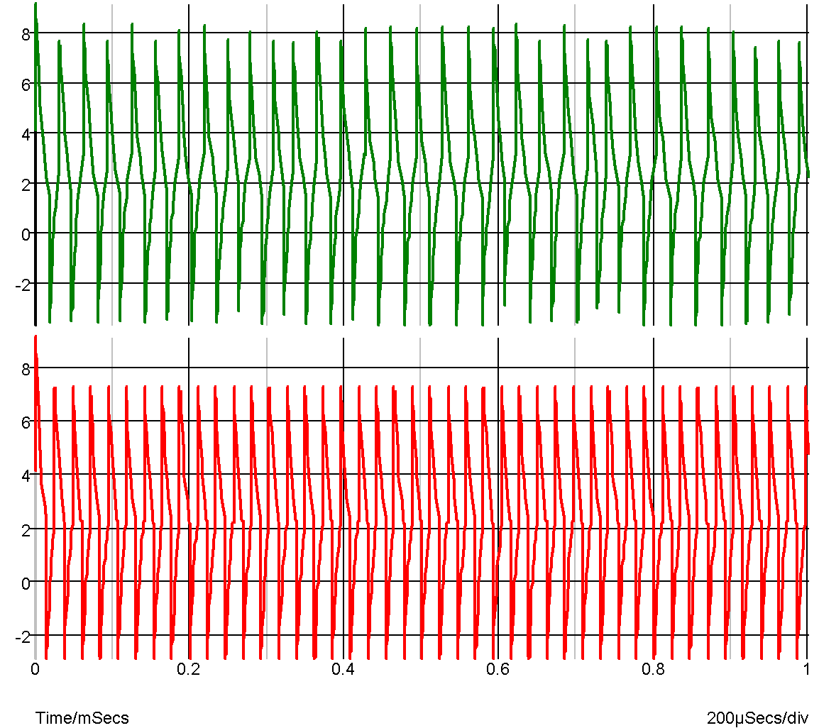
The top trace is without threshold control and the bottom trace is with it.
Digital-Analog Interface Bridge
Netlist entry
Axxxx in out model_name
Connection details
| Name | Description | Flow | Type |
| in | Input | in | d |
| out | Output | inout | g |
Model format
.MODEL model_name dac_bridge parameters
Model parameters
| Name | Description | Type | Default | Limits |
| out_low | Analog output for 'ZERO' digital input | real | 0 | none |
| out_high | Analog output for 'ONE' digital input | real | 5 | none |
| g_resistive | Output conductance for 'RESISTIVE' digital input | real | 0.001 | none |
| g_pullup | Output conductance for 'STRONG' digital high input | real | 0.01 | none |
| g_pulldown | Output conductance for 'STRONG' digital low input | real | 0.01 | none |
| g_hiz | Output conductance for 'HI_IMPEDANCE' strength | real | 1.00E-09 | none |
| input_load | Capacitive input load (F) | real | 1pF | none |
| t_rise | Rise time 0 -> 1 | real | 1nS | ???MATH???1\text{e}^{-12} - \infty???MATH??? |
| t_fall | Fall time 1 -> 0 | real | 1nS | ???MATH???1\text{e}^{-12} - \infty???MATH??? |
| knee_high | Knee voltage logic high state | real | 3 | none |
| knee_low | Knee voltage logic low | real | 2 | none |
| sink_current | Input sink current | real | 0 | none |
| source_current | Input source current | real | 0 | none |
| v_smooth | Smoothing function offset voltage | real | 0 | ???MATH???0 - \infty???MATH??? |
| in_family | See Family parameters | string | UNIV | none |
| vsupply_nominal | nominal supply voltage, used to scale output levels if vsupply parameter provided by connected digital device identified by interface_model parameter | real | 5.0 | ???MATH???0 - \infty???MATH??? |
| technology | Technology, e.g. HC, LVC etc. This has no effect on device operation. It is used by the user interface to group bridge models | string | none | |
| description | Sub-type to technology, e.g. schmitt, buffer, standard. This has no effect on device operation. It is used by the user interface to identify bridge characteristics | string | none |
Instance parameters
| Name | Description | Type | Default | Limits |
| interface_model | Model of device connected to bridge. Used to retrieve vsupply parameter of device if present. In normal operation using implicit bridge devices, this parameter is set automatically by the simulator | string | none | |
| inactive | if non-zero, output will present a 1Ohm resistor to ground. This parameter is used internally to create dummy instances for the purpose of analysing logic compatibility | integer | 0 | none |
DC characteristics
This digital to analog interface bridge is the main device used to connect digital signals to analog devices. The output provides an analog voltage and source resistance according to the state and strength of the driving digital input. The output has a non-linear characteristic that is a simplified model of a typical digital output stage. The following graphs show the output characteristics for the supplied high speed CMOS DA bridge. This has the following model parameters:
.model HC_dac dac_bridge
+ out_high=5         ; Logic high voltage
+ input_load=-31p    ; Compensates for added rise and fall time
+ t_rise=2n          ; Output rise time
+ t_fall=2n          ; Output fall time
+ g_pullup=0.024     ; 1/(logic high output resistance)
+ g_pulldown=0.034   ; 1/(logic low output resistance)
+ g_hiz=1e-9         ; 1/(high impedance output res)
+ knee_low = 2.0     ; voltage at resistive/constant current
+                    ; knee logic low
+ knee_high =2.75    ; voltage at resistive/constant current
+                    ; knee logic high
+ v_smooth = 0.5     ; Knee smoothing band
+ in_family="HC"
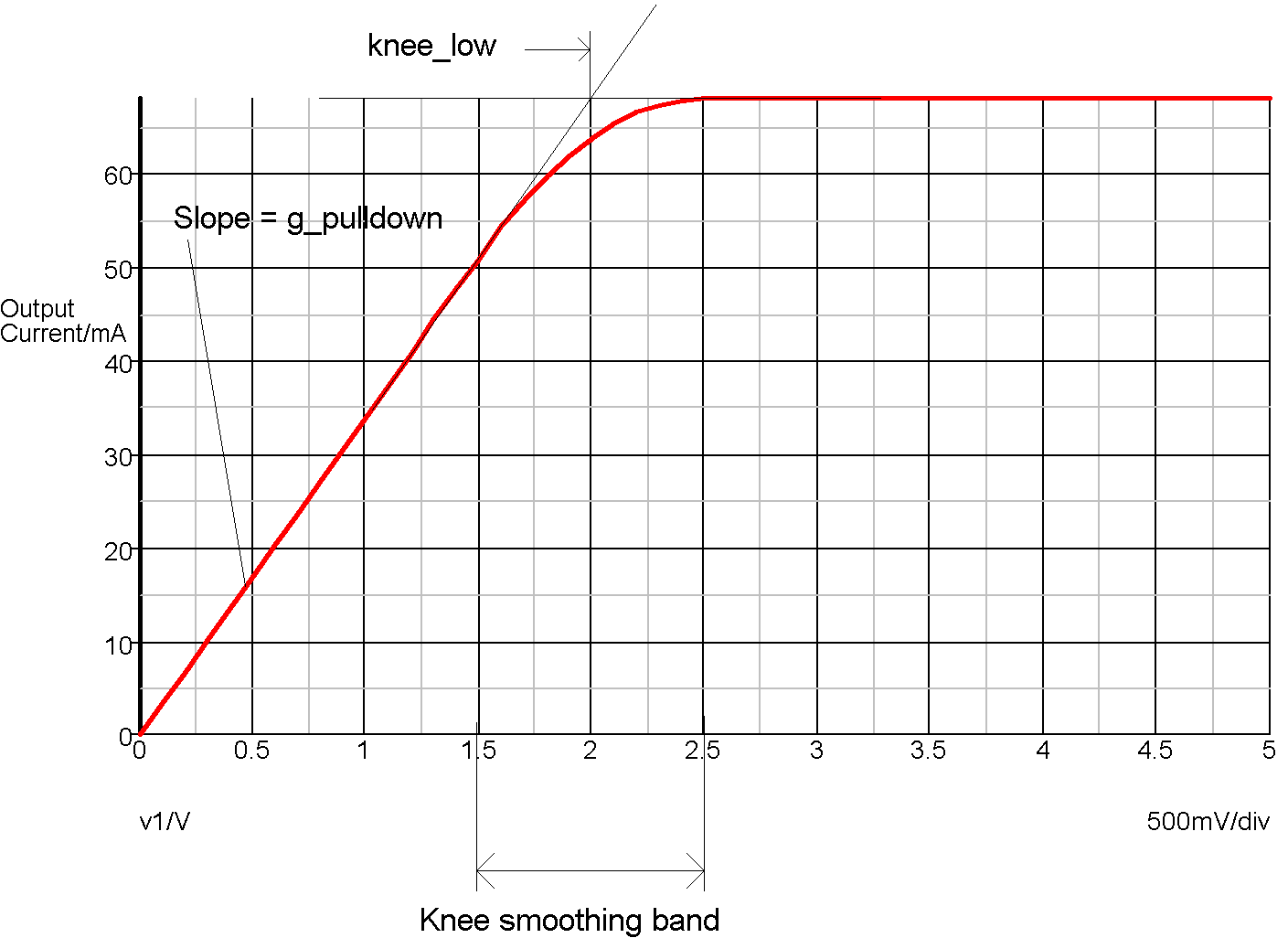
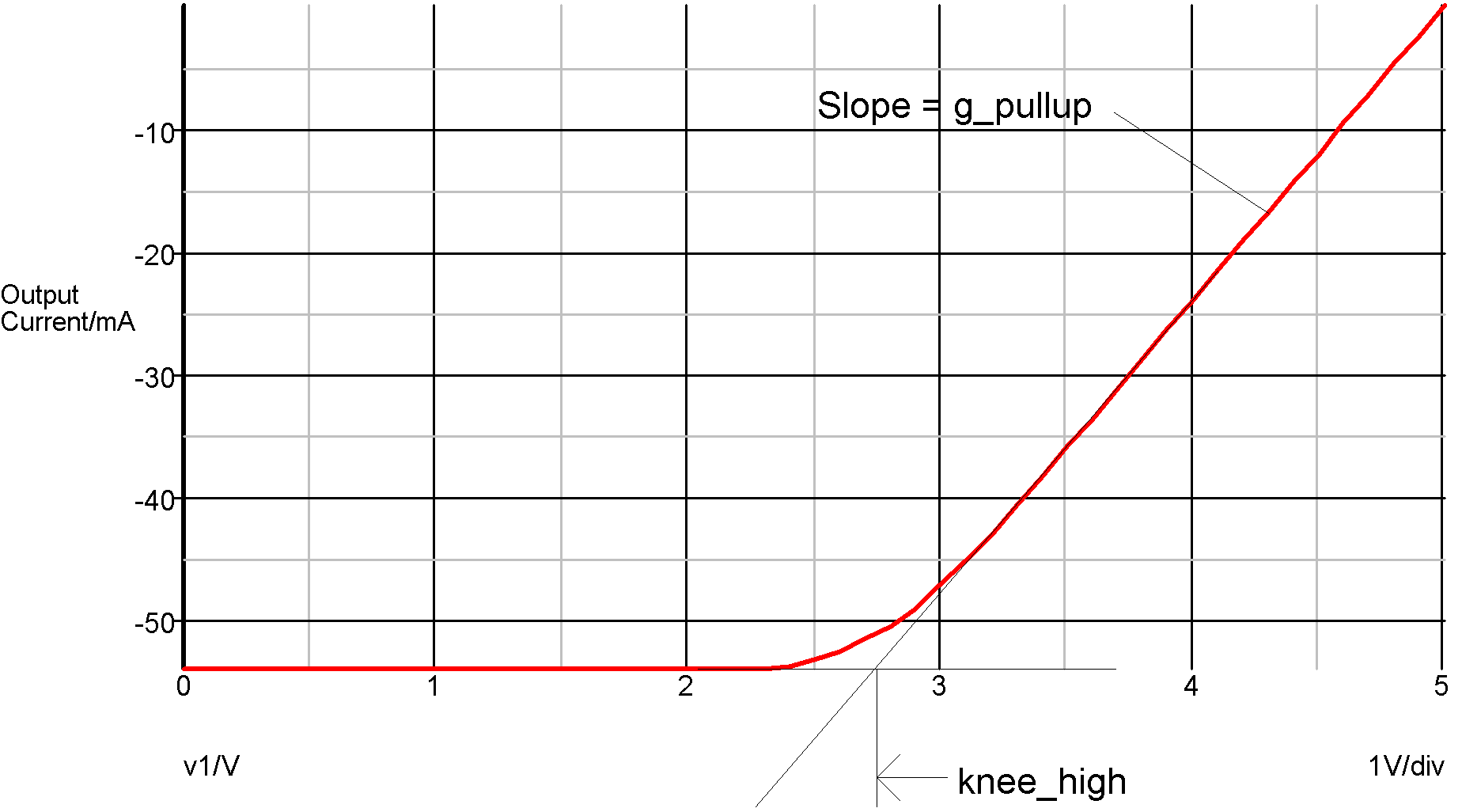
Logic '0' state - strength = STRONG
In the above graph, the slope of the curve at V=0 is determined by the G_PULLDOWN parameter. The 'knee smoothing band' is a transitional area where the output switches from a constant resistance to a constant current. The smoothing characteristic is a quadratic and is calculated to be smooth at all points. This is required for good convergence behaviour. The knee smoothing band starts at KNEE_LOW-V_SMOOTH and finishes at KNEE_LOW+V_SMOOTH.
Logic '1' state - strength = STRONG
If a state with RESISTIVE strength is applied to the input of a digital to analog interface bridge, the output has the characteristic of a pure resistor connected to the voltage associated with the input's state. In the example given above, this would be a 1k resistor connected to 0V for the logic '0' state and a 1k resistor connected to +5V for the logic '1' state. (1k is 1/G_RESISTIVE)
For the HI-IMPEDANCE strength, the output will look like a resistor of value 1/G_HIZ connected to a voltage half way between the two analog output states. (1G connected to 2.5V in the above example.)
When the input state is UNKNOWN the output will be as if it were half way between the two known states. This is a compromise solution. The UNKNOWN state does not have a parallel in the analog domain so instead it is treated as a transitional state. In some cases the UNKNOWN state occurs in transitional cases although this is not the correct meaning of UNKNOWN.
If the interface_model parameter is present, the referenced model will be examined for a vsupply parameter and an out_res parameter. If vsupply is present, this will scale the output levels by a factor of vsupply/vsupply_nominal. If out_res is present, this will set a default value of 1/out_res for each of the parameters the g_pulldown and g_pullup.
Switching Characteristics
When the logic state at the input changes, the output will transition from the current state to the target state in a time determined by T_RISE or T_FALL according to the direction of the state change.
Analog-Digital Schmitt Trigger
Netlist entry
Axxxx in out model_name
Connection details
| Name | Description | Flow | Type | Allowed types |
| in | Input | inout | g | g, gd |
| out | Output | out | d | d |
Model format
.MODEL model_name adc_schmitt parameters
Model parameters
| Name | Description | Type | Default | Limits | ||
| in_low | Maximum 0-valued analog input | real | 0.1 | none | ||
| in_high | Minimum 1-valued analog input | real | 0.9 | none | ||
| rise_delay | Rise delay | real | 1nS | ???MATH???1\text{e}^{-12} - \infty???MATH??? | ||
| fall_delay | Fall delay | real | 1nS | ???MATH???1\text{e}^{-12} - \infty???MATH??? | ||
| time_tol | Threshold time tolerance | real | 100pS | ???MATH???1\text{e}^{-12} - \infty???MATH??? | ||
| out_low | Analog out for 'ZERO' input | real | 0 | none | ||
| out_high | Analog output 'ONE' input | real | 5 | none | ||
| clamp_res | Clamp minimum resistance | real | 1 | 1e-06 ???MATH???- \infty???MATH??? | ||
| clamp_bias | Clamp voltage | real | 0.8 | 0.2 - 2 | ||
| out_family | See Family parameters | string | UNIV | none | ||
| vsupply_nominal | nominal supply voltage, used to scale thresholds if vsupply parameter provided by connected digital device | real | 5.0 | ???MATH???0 - \infty???MATH??? | ||
| init_cond | Initial condition | real | 0 | none | ||
| technology | Technology, e.g. HC, LVC etc. This has no effect on device operation. It is used by the user interface to group bridge models | string | none | |||
| description | Sub-type to technology, e.g. schmitt, buffer, standard. This has no effect on device operation. It is used by the user interface to identify bridge characteristics | string | none |
Instance parameters
| Name | Description | Type | Default | Limits |
| interface_model | Model of device connected to bridge. Used to retrieve vsupply parameter of device if present. In normal operation using implicit bridge devices, this parameter is set automatically by the simulator | string | none | |
| inactive | if non-zero, device will output Hi-Z and present a 1Ohm input to ground. This parameter is used internally to create dummy instances for the purpose of analysing logic compatibility | integer | 0 | none |
Device Operation
This device is identical to the Analog-Digital Interface Bridge except for one difference. That is the behaviour of the device when the analog input lies between the threshold voltages. With the interface bridge, the output is UNKNOWN under these circumstances but with this Schmitt Trigger, the output retains its previous value and so is always in a known state. In summary, the output will only switch from low to high when the input exceeds the higher threshold (IN_HIGH) and will only switch from high to low when the input descends below the lower threshold (IN_LOW).
If initial input voltage lies between the hysteresis thresholds, the output state is determined by the init_cond parameter.
If the interface_model parameter is present, and the referenced model has a vsupply parameter, the input thresholds are scaled by a factor of vsupply/vsupply_nominal. This feature allows the supply voltage for each digital device to be customised
| ◄ Sources | Functions ▶ |