6.1.3 Constant Voltage Subcircuit
To download the examples for Module 6, click Module_6_Examples.zip
In this topic:
What You Will Learn
This topic creates a constant voltage load using a procedure similar to the one used in 6.1.2 Constant Current Subcircuit. This topic is marked optional only for time reasons, not because the load type is not useful. Constant voltage loads are useful to test current sourced converters such as LED drivers, or for testing the current limit behavior of a voltage-sourced converter.
- How to create a constant voltage subcircuit load using a Piecewise Linear (PWL) Resistor.
- That constant voltage loads should have a series resistance
Model Requirements
The constant voltage load should:
- Model a high resistance for voltages below the constant voltage limit, and a constant voltage for currents above some minimum current value.
- Include a parasitic series resistance.
- Limit the valid parameter values, including the calculated parameter values, to a range of values.
- Include a basic parameter editing dialog.
- Be self-contained in a schematic component file.
Model Design Procedure
The design procedure for this model is broken into three logical parts.
- Part #1: Change PWL Resistor Type and Rename Constant Current Load File
- Part #2: Parametrize the PWL Resistor
- Part #3: Define Calculated Parameters
- Part #4: Check Passed Parameter Values With dot error
Part #1: Change PWL Resistor Type and Rename Constant Current Load File
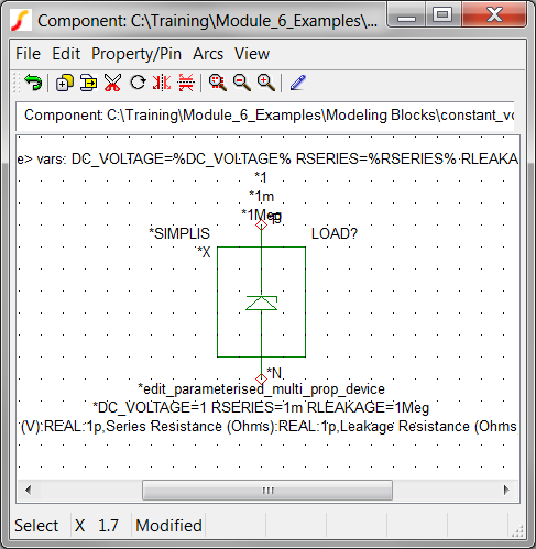
You will start the model by opening the constant_current_load.sxcmp file you created in the 6.1.2 Constant Current Subcircuit topic. You will then learn a clever trick to modify the PWL resistor type to a Current controlled PWL resistor (IPWL) and save this schematic component to a new file.
- Open the constant_current_load.sxcmp schematic component created during the 6.1.2 Constant Current Subcircuit topic. If you haven't created this file, open the "answer" file : 6.1.1_constant_current_load_answer.sxcmp.
- Select R1, the Voltage controlled PWL resistor.
- Right click and select the Edit/Add Properties... menu option. Result: The Edit Properties dialog appears.
- Double click on the SIMPLIS_TEMPLATE property. Result: The Edit Property dialog for the SIMPLIS_TEMPLATE opens:
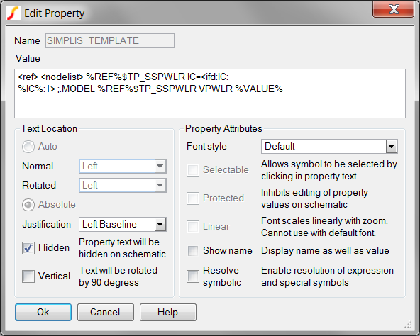
- Carefully edit the SIMPLIS_TEMPLATE, changing the V PWLR text to I
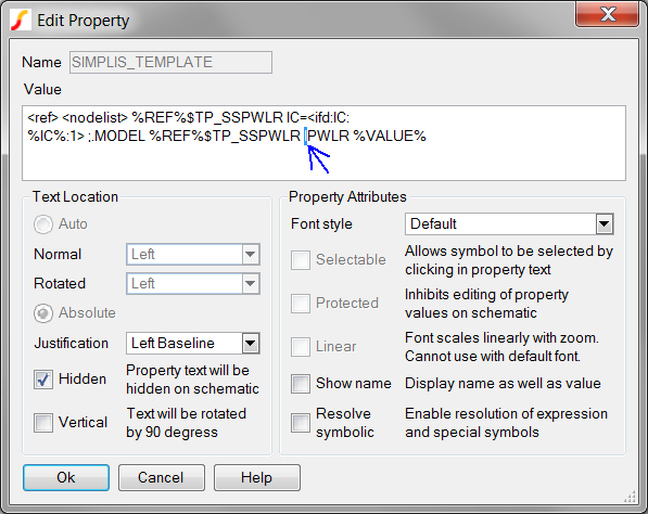
PWLR. Note: This text is at the end of the SIMPLIS_TEMPLATE property value, just before the %VALUE% text.Result: The changed SIMPLIS_TEMPLATE value appears as below.
- Click Ok on the Edit Property and then click Ok on the Edit Properties dialog to save your changes.
- Double click on the R1 resistor symbol to open the parameter editing
dialog. Note the caption should read Define IPWL Resistor: R1.
- Click Cancel on the dialog.
- From the Schematic Editor menu, select File ▶ Save As...
- Enter constant_voltage_load.sxcmp in the File name field and click Save to save the schematic component.
Part #2: Parametrize the PWL Resistor
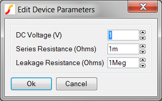
In this part, you will define the PWL resistor points using parameter values. The constant voltage load requires three parameters which the user will enter on the parameter editing dialog. These parameter names and the default values are shown in the table below:
| Parameter Description | Parameter Name | Default Parameter Value |
| The constant load voltage in volts | DC_VOLTAGE | 1 |
| The leakage resistance in ohms | RLEAKAGE | 1Meg |
| The series resistance in ohms | RSERIES | 1m |
There are several ways to add these parameters to the actual PWL resistor. For this model you will define parameters calculated in the F11 window in addition to the parameters passed into the subcircuit through the symbol. In addition to the three parameters passed into the subcircuit through the symbol, the following three calculated parameters will be used:
| Parameter Description | Parameter Name |
| Second current point | CURRENT_2 |
| Third voltage point | VOLTAGE_3 |
| Third current point | CURRENT_3 |
The resulting V-I curve for the load with the parameters annotated is shown below. Each voltage-current pair is annotated in (x,y) format. How the four additional parameters are calculated will be covered in Part 3: Define Calculated Parameters.
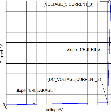
Notice the last segment in the resistor has a positive, but not infinite slope. SIMPLIS requires all PWL resistors to have positive slope for both the first and last PWL segment, and this model allows users to define the load as a ideal voltage source. If you did not add this third segment, the model would produce an error message because the slope of the last segment would be zero. This segment is placed at a voltage which is well beyond the operating voltage range of the load, preventing the final segment from effecting the normal operation of the load.
To parameterize the PWL resistor,
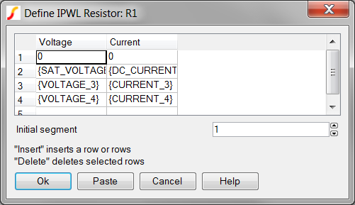
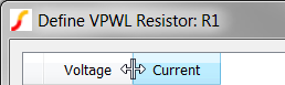
- Double click on the PWL resistor R1. Result: The Define VPWL Resistor: R1 dialog opens:
- Stretch the Voltage and Voltage columns to approximately twice the
default width.
- Position the mouse between the Voltage and Current Columns on
the title bar row. Result: The mouse cursor changes to two vertical bars, indicating the columns are ready to be resized.
- Press and hold the left mouse button and drag the column to resize.
- Repeat for the Current column by moving the mouse cursor to the right of the Current column, and repeating step B.
- Position the mouse between the Voltage and Current Columns on
the title bar row.
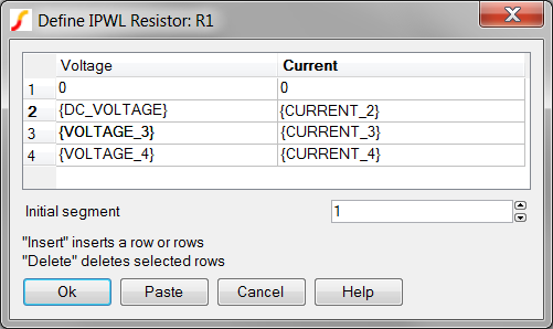
- Edit the second data point:
- Replace {SAT_VOLTAGE} with {DC_VOLTAGE}.
- Replace {DC_CURRENT} with {CURRENT_2}. Result: The dialog should appear as follows:
 CAUTION:Spelling errors here will have disastrous consequences later on. Whenever you enter text by hand, double check the spelling. A good way to avoid spelling errors is to copy and paste the text from this document.
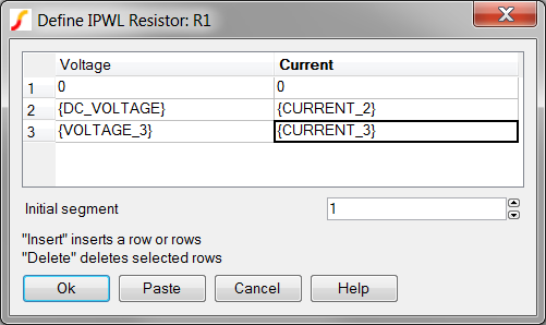
- To delete the fourth row:
- In Row 4, select either the Voltage or Current cell.
- Press the Delete key to remove the data point. Result: The final dialog should appear as follows:
- Click Ok to save the changes.
At this point, the PWL resistor uses four parameters - one is passed in from the symbol, and the other three are calculated from the passed-in parameters. In the next part, you will define the four calculated parameters in the F11 window of the constant_voltage_load.sxcmp schematic component.
Part #3: Define Calculated Parameters
Both the second and third points are calculated from the parameters passed into the subcircuit. In this part, you will define these parameters in the F11 window of the schematic component.
The constant current load designed in topic 6.1.2 Constant Current Subcircuit, has an infinite output impedance when the USE_RSHUNT parameter is false. As a result, the PWL resistor definition required a third segment to guarantee the last segment has a positive, but finite slope. The constant voltage load design has a finite, non-zero series resistance. Although this resistance is not required, the simulator will produce errors when an ideal voltage source is placed across an ideal capacitor. An ideal voltage controlled PWL resistor has an ideal voltage source behavior, and therefore adding a small series resistance will make the model easier to use. Because the last segment is a finite resistance, the PWL resistor definition requires two segments - the leakage segment and the voltage-clamping segment.
To assign values for these segments:
- Press F11 to open the command (F11) window.
- Select all text in the F11 window and delete it.
- The second current point is set by parameter CURRENT_2 and is simply the
ratio of the DC_VOLTAGE over the RLEAKAGE. Enter the following text in the F11
window of the schematic:
.VAR CURRENT_2 = { DC_VOLTAGE / RLEAKAGE }Notice: The final segment is defined by the slope of the resistance RSERIES. SIMPLIS views PWL resistors as a series of slopes - when the simulation voltage or current exceeds the last numerical voltage or current point defined by the resistor, SIMPLIS assumes the resistance is unchanged from the last segment. This means that you can very simply define the CURRENT_3 parameter to be one amp greater than the CURRENT_2 parameter, and the VOLTAGE_3 parameter to be RSERIES volts greater than the DC_VOLTAGE parameter. When the load current exceeds the CURRENT_3 parameter, SIMPLIS will continue to use the RSERIES resistance defined for the resistor. - Enter the following text in the F11 window of the schematic:
.VAR CURRENT_3 = { CURRENT_2 + 1 }
.VAR VOLTAGE_3 = { DC_VOLTAGE + 1 * RSERIES }
At this point, all PWL resistor points are defined, but no error checking has been added. In the next step, Part_4:_Check_Passed_Parameter_Values_With_dot_error, you will add error checking for the parameter values.
Part #4: Check Passed Parameter Values With .ERROR
In this part you will use the .IF/.ENDIF and .ERROR constructs to check if the parameter values are within the ranges allowed by the model.
- Each error message tests the passed parameters are greater than zero. Copy the
following three error messages and paste into the F11 window.
.IF { DC_VOLTAGE <= 0 }
    .ERROR "The dc load voltage parameter (DC_VOLTAGE) for the constant_voltage_load subcircuit must be greater than 0."
.ENDIF

.IF { RSERIES <= 0 }
    .ERROR "The series resistance parameter (RSERIES) for the constant_Voltage_load subcircuit must be greater than 0."
.ENDIF

.IF { RLEAKAGE <= 0 }
    .ERROR "The leakage resistance parameter (RLEAKAGE) for the constant_Voltage_load subcircuit must be greater than 0."
 .ENDIF
Symbol Design Procedure
As in Symbol_Design_Procedure" section 6.1.1 Symbol Design Procedure, the symbol design procedure is broken into two parts:
Part #1: Assign and Edit a Symbol
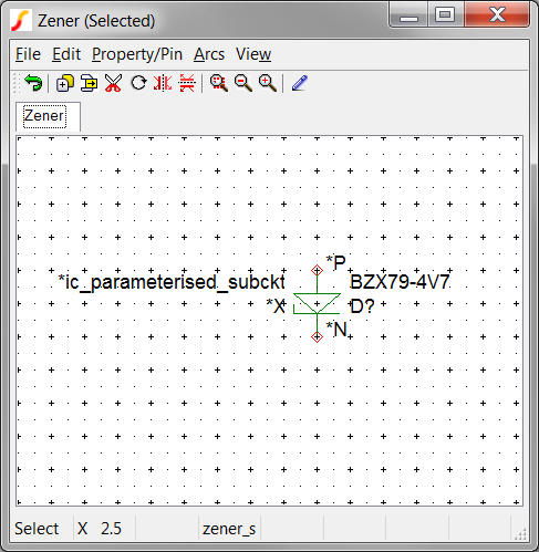
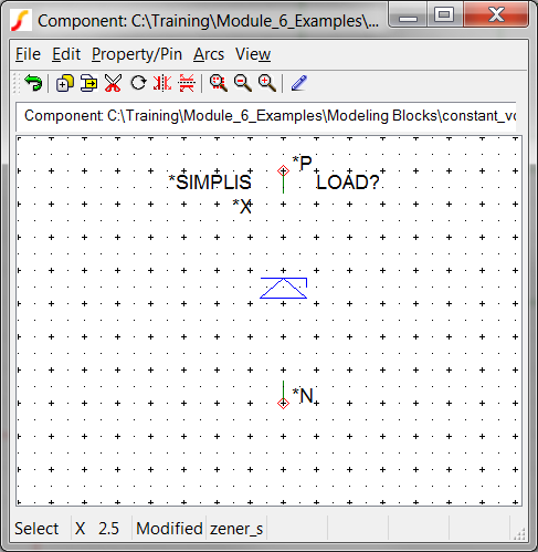
At this point, the constant voltage load has a complete schematic but no symbol. Since the load is essentially a high impedance until the voltage limit is reached, it behaves as a Zener diode, and this will be the symbol assigned to the load. The simplest way to do this is to copy the global symbol for the Zener diode to the schematic component. You will then modify the graphical elements of the symbol to indicate that the underlying model is not the built-in Zener diode.
- Press Z to place a Zener diode on the schematic. Click the Ok button to extract the parameters.
- Select D1, the Zener diode symbol you just placed.
- Right click and select Edit Symbol...
Result: The global symbol for the Zener diode opens in the symbol editor:
 Important: It is very important to save this symbol to your schematic component file before you start to edit it. If you make edits to this symbol and inadvertently save them, those changes would be applied to the global current souce symbol used by other schematics. This could have disastrous effects in other schematics.
 - To save the symbol to your schematic component file,
- Select the Symbol Editor menu File ▶ Save...
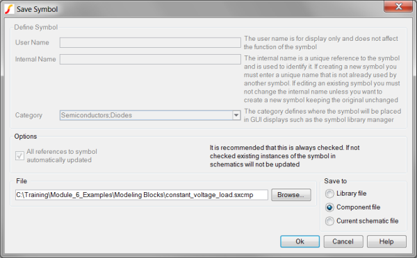
Result: The Save Symbol dialog opens
- In the Save to radio button group, select Component file.
- Click the Browse... button to navigate the file system and select
the schematic component file for the constant_voltage_load.sxcmp. The
configured dialog will appear as follows:
- Select the Symbol Editor menu File ▶ Save...
- To delete unneeded symbol properties INITSCRIPT and VALUE:
- Position the mouse over the *ic_parameterised_subckt text and left
click once. This text is the property value of the INITSCRIPT
property. Result: The text changes color from black to blue, indicating the property is selected.
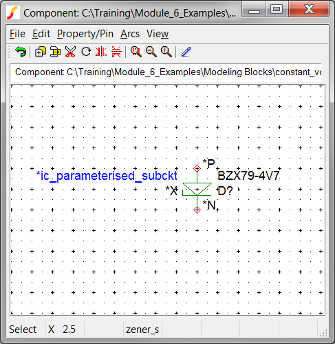
- Press the Delete key to delete the property.
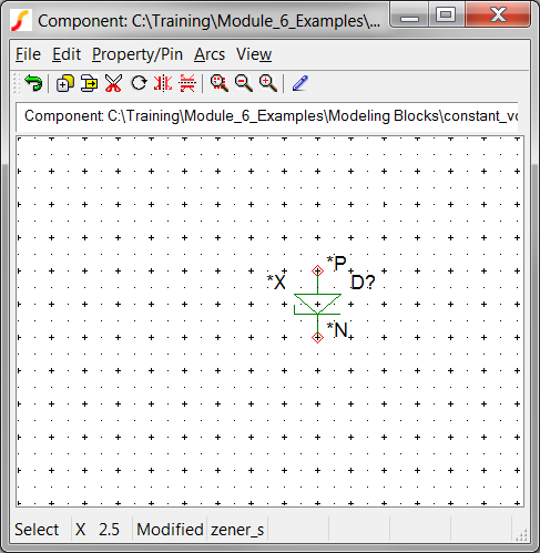
- Repeat for the text BZX79-4V7 which represents the VALUE
symbol property. Result: At this point the symbol editor should appear as follows:
- Position the mouse over the *ic_parameterised_subckt text and left
click once. This text is the property value of the INITSCRIPT
property.
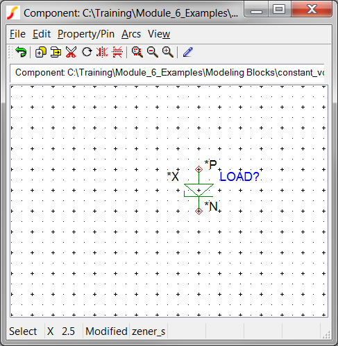
- To change the REF property to LOAD?:
- Select the D? text and Press F7 to edit the REF property.
- Enter a Value of LOAD? in the In the Edit Property dialog. Result: The symbol now appears as follows:
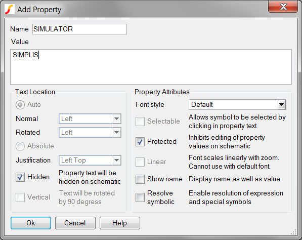
- To add a SIMULATOR property and set value to SIMPLIS:
- From the Symbol Editor window select the menu item Property/Pin ▶ Add Property...
Result: The Add Property dialog opens
- In the Name field, enter SIMULATOR.
- In the Value field, enter SIMPLIS.
- Check the Protected and Hidden check boxes. Result: The configured Add Property dialog appears as follows:
- From the Symbol Editor window select the menu item Property/Pin ▶ Add Property...
- Click Ok to add the symbol property.
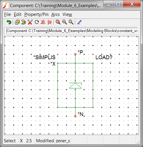
- Next, to modify the graphical representation so users will know this symbol does
not represent the built-in current source model, follow these steps:
- Position the mouse over the N pin, then press and hold the mouse button
while dragging the pin downwards two major grid ticks. Result: The N pin is now two grid ticks down from the original position.
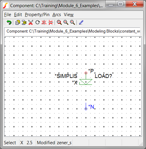
- Repeat for the P pin, moving the pin up three grid ticks. Unlike the
current source symbol you modified in the last topic, the pins on the zener
symbol are two grid ticks closer. Result: The P pin is now three grid ticks up from the original location.
- Position the mouse over the N pin, then press and hold the mouse button
while dragging the pin downwards two major grid ticks.
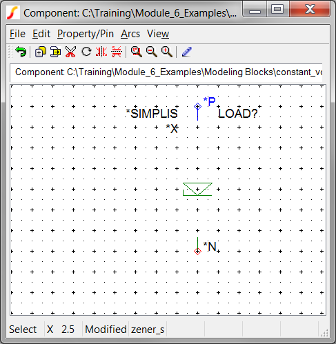
- To rotate the zener portion of the symbol and move it up 1/2 a major grid tick to
center the zener portion vertically between the pins:
- Press and hold the left mouse button and drag the mouse to draw a selection
box over the zener portion in the middle of the symbol:
- Release the mouse butto.Result: The zener graphical elements are selected.
- Press F5 twice to rotate the selected graphical elements. Click on
the selected items and drag the selected items up approximately 1/2 a major
grid tick. Note - you may need to zoom in to center the graphical elements.
Result: The zener graphical elements are centered between the two pins.
- Press and hold the left mouse button and drag the mouse to draw a selection
box over the zener portion in the middle of the symbol:
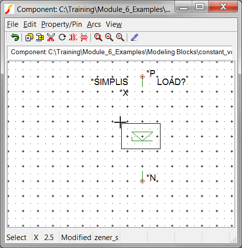
- To connect the pins to the zener and add a graphical box around the zener:
- Double click to start a graphical "wire" segment.
- Left click once to define a corner or end point.
- Right click to stop wiring.
- If you make a mistake, right click to stop wiring and press Ctrl-Z
to undo. Result: The symbol should appear approximately as follows:
- Select the Symbol Editor menu File ▶ Save... to save the symbol to the schematic component file.
- Navigate to the SIMetrix/SIMPLIS Schematic Editor window. Select and delete the Zener diode D1.
You now have a symbol which will call the subcircuit based constant voltage load model. The functionality of the underlying subcircuit is implied by the Zener diode symbol, and the box around the Zener diode source suggests to the user that this is not a normal Zener diode. At this point the symbol doesn't pass parameters to the underlying subcircuit, nor does the symbol have a parameter editing dialog. In the next part, Part_2:_Add_Parameters_and_Dialog_Properties, you will use a spreadsheet to add the required symbol properties.
Part #2: Add Parameters and Dialog Properties
Included in the Module_6_Examples.zip file is a pre-prepared dialog definition spreadsheet similar to the one used in the previous module. Like the spreadsheet used in 6.1.1 Constant Resistance Subcircuit, this spreadsheet contains all script commands to add the properties to the symbol. The extracted file is located at: C:\Training\Module_6_Examples\6.1.3_constant_voltage_load_dialog_definition_worksheet.xlsx. The dialog definition creates the following dialog for the constant voltage load:
To add the symbol properties,
- Open the 6.1.3_constant_voltage_load_dialog_definition_worksheet.xlsx excel spreadsheet.
- Copy the 7 cells: B23-B31 to the windows clipboard.
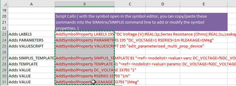
- Navigate to the SIMetrix/SIMPLIS command shell window.
- Click the mouse in the command line entry located at the top of the command shell
window:
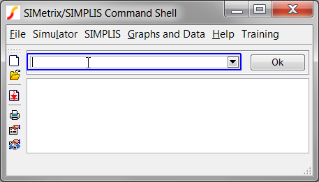
- Press Ctrl+V to paste the commands in the command line.Result: the last command is partially visible in the command line.
- Press Enter or click the Ok Button on the command line.Result: The commands are executed in SIMetrix/SIMPLIS. Each AddSymbolProperty command adds a single symbol property to the symbol. As in previous exercises, the dialog definition properties are protected. All properties are hidden from view when the symbol is placed on the parent schematic.
- Select the Symbol Editor menu File ▶ Save... to save the symbol to the schematic component file.
The model and symbol are now complete and ready for testing.
Test the Model
Now that the model and associated symbol are completed, its time to start testing. A testbench schematic for the constant current load is located in the Module_6_Examples directory. After you place the load, this test schematic is ready to simulate. You will then run a few experiments on the model to verify it works as expected.
To start testing the model,
- Open the 6.3_test_constant_voltage.sxsch schematic.Result: The testbench schematic opens, this schematic has been specially prepared to test the load including two XY probes and a ramped current source. Each X-Y probe is configured to display one of the two PWL resistor operating segments.
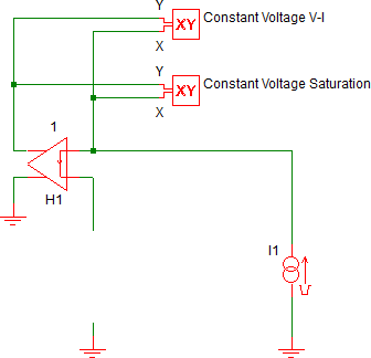
- From the Schematic Editor menu, select Hierarchy ▶ Place Component (Relative Path)...
- Select the constant_voltage_load.sxcmp component file from the Modeling Blocks directory.
- Place the load on the schematic where the opening below H1 is located.
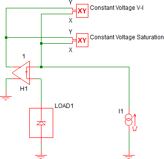
- Press F9 to run the simulation. Result: The V-I curves for the load are generated on three tabs. The current tab displays the saturation characteristics of the load:
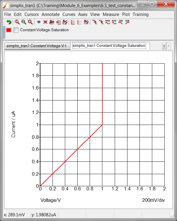
At this point the constant voltage load is ready for some experiments to test the load's behavior.
Experiment #1: Test Dialog and Change Parameter Values
Whenever you pass parameters to subcircuits, it is important to test that the parameters are being passed properly and the simulation results reflect the actual parameter value. In this experiment, you will change the load parameters and verify the value changes in the simulation.
- Navigate to the Schematic Editor window.
- Double click on the subcircuit load symbol to edit the resistance parameter.
Result: The parameter editing dialog opens.
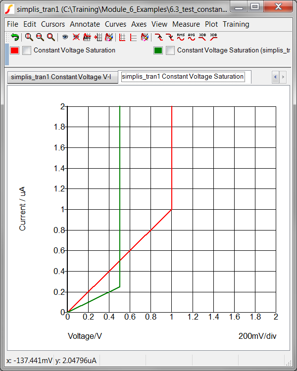
- To change the parameters:
- Change the DC Voltage value to 500m.
- Change the Series Resistance parameter to 10m.
- Change the Leakage Resistance to 2Meg. Result: The dialog should appear as follows.
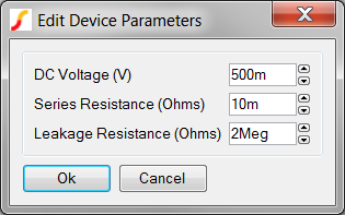 Click Ok to accept the dialog.
- Press F9 to run the simulation. Result: The green V-I curve for the load is generated with the new parameters.
The output curves clearly reflect the changed parameter values.
Experiment #2: Test .ERROR Message
Testing the .ERROR message is slightly more difficult because the parameter editing dialog will not allow you to enter an invalid value. Instead you will manually edit the value using the Edit Properties dialog.
- Select the LOAD1 symbol.
- Right click and select the Edit/Add Properties... menu option. Result: The Edit Properties dialog opens.
- To change the DC_VOLTAGE, RSERIES, and RLEAKAGE properties
to 0:
- Double click on each property. On the Edit Property dialog, change each property Value to 0, and click Ok on the Edit Property dialog to accept the changes.
- Repeat for each property.
- Click Ok on the Edit Properties dialog.
- Press F9 to run the simulation.Result: All three parameters are less than the minimum limit specified in the F11 window of the constant_voltage_load.sxcmp schematic, and each .ERROR statement is output to the command shell:
*** ERROR *** (6.3_test_constant_voltage.net): Subckt def constant_voltage_load used by X$LOAD1:
The leakage resistance parameter (RLEAKAGE) for the constant_Voltage_load subcircuit must be greater than 0.
*** ERROR *** (6.3_test_constant_voltage.net): Subckt def constant_voltage_load used by X$LOAD1:
The series resistance parameter (RSERIES) for the constant_Voltage_load subcircuit must be greater than 0.
*** ERROR *** (6.3_test_constant_voltage.net): Subckt def constant_voltage_load used by X$LOAD1:
The dc load voltage parameter (DC_VOLTAGE) for the constant_voltage_load subcircuit must be greater than 0.
*** ERROR *** (6.3_test_constant_voltage.net): Could not evaluate "CURRENT_3= CURRENT_2 + 1 "
Cannot find vector of name 'CURRENT_2'
*** ERROR *** (6.3_test_constant_voltage.net): Could not evaluate "CURRENT_2= DC_VOLTAGE/RLEAKAGE "
Arguments out of range for operator '/'
Experiment #3: Test Minimum Values Allowed by Dialog
In the previous experiment you set the load parameters to values less than the minimum allowed by the parameter editing dialog. In this short experiment you will verify the dialog prevents users from entering values less than the specified minimum value.
- Double click on the LOAD1 symbol to open the parameter editing dialog.
Result: Although the three parameters were set to 0 in the last exercise, the dialog automatically changes the values to the minimum values allowed for each parameter. Each minimum value is defined in the excel spreadsheet for this dialog definition.
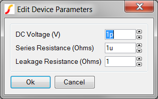
- Press the up arrow button on the DC Voltage spinner control. Result: The DC Current value changes from 1p to 2p .
- Press the down arrow button twice on the DC Voltage spinner control. Result: The DC Current value changes from 2p to 1p , and on the second click, the minimum value of 1p is enforced.
Conclusions and Key Points to Remember
A PWL resistor can be used to define a very flexible constant voltage load. This load simulates a low impedance voltage clamp, similar to a precise Zener diode.
Key points to remember are:
- You can define parameters local to the F11 window. These parameters can be constants or be defined in terms of the parameters passed into the subcircuit.
- Ideal voltage sources, such as an ideal voltage controlled PWL resistor will produce simulator errors if places in parallel with an ideal capacitor.
- You can validate parameter values are within a range with the .ERROR statement. Any parameter can be checked, including calculated parameters.
- When parametrizing PWL resistors, make certain the first and last segments have a positive slope.